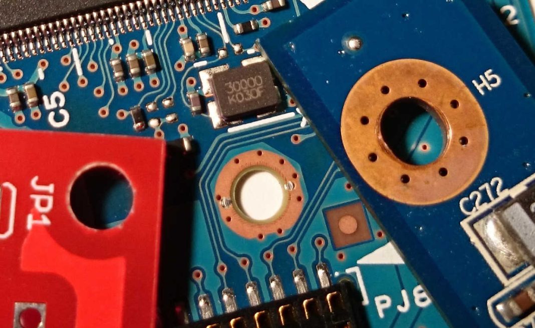
The PCB manufacturing process includes fine process processes such as cutting, grinding, filming, exposure, development, etching and plating, lamination, drilling pcb holes, surface treatment and solder mask. Strict control of each link can ensure the normal operation of the PCB. JHD’s one-stop ISO9001:2015 quality management system production line strictly implements high-standard production for each process. In this article, we will take you to learn more about all types of pcb vias.
Through Holes and Tool Holes:
Most printed circuit boards have drilling pcb holes. Many kinds of holes are described below:Older PCB technologies mainly support lead assemblies that require one hole per pin, called “through hole” or “PTH” (plated through hole) technologies, but more and more modern technologies use dense surface mount components. We name this technology “SMT” or “surface mount technology”. The main differences between them are the number, size, and use of holes. Note that PTH and SMT components can be mixed assembled freely on the board. The types of holes are first divided into through holes and tool holes:
1) Through-Hole:
This term doesn’t need much definition, as its name says it all, although today’s technology does include scalability with only a fraction of through-holes (so-called “blind vias”) on a circuit board. A through-hole is a hole that goes through the circuit board. They are usually plated through, so there is a conductive path from one side to the other ( they are also called “plated through holes” or “PTHs” when plated through).
Through-hole technology, also known as “through-hole,” refers to a hole that goes completely through a circuit board. They are divided to plated (PTH) and non-plated (NPTH).
Both PTH and NPTH have their own characteristics and uses, and it is recommended to understand their differences before starting a PCB design project.
A. Plated Slot Holes (PTH):
The main feature of this type of hole is that, during the manufacturing process, after drilling the plate, a thin layer of copper is plated on the hole wall to make the hole conductive. In this way, the connection between component leads and copper wires has lower resistance and better mechanical stability after PCB assembly is complete.
Today, we use double-sided and multi-layered PCBs more most widely, and some through-holes are plated so as to connect components to the any layers in the board.
B. Non-Plated Slot Hole (NPTH):
As its name says, in this type of through hole, there is no copper plating on the hole walls, so the hole barrel has no electrical properties. When copper wires are printed on only one side of a PCB, they are very popular, but as the number of layers in a PCB increases, their use decreases.The main advantage of NPTH is that its manufacturing process is simpler and significantly faster. Today, they are often (but not limited to) used as tool / mounting holes: to secure the PCB to its operating position. However, they can also be used to install components.
2) Tool Hole:
Also called “mounting hole”, it refers to a hole in the pcb for connecting the circuit board to the test fixture or its operating position. Generally, tool holes are not plated, which means that they are insulated from any electrical components or traces on the pcb board.
Holes have implicit interactions with every PCB layer which they pass through. When plated through holes carrying signals pass through the ground plane, use (negative) gap pads to ensure good separation of the copper ground plane from the passing signals. Power plane layers use similar clearance pads. The diameter of the gap pad must be larger than the drilled hole (about 15 mils).
Blind and Buried Vias
With the development of science and technology, PCB has developed from single panel to double-sided and multi-layer, and its application is becoming wider and wider. What are so many small holes on double-sided board and multi-layer board and what are the benefits of so many designs? Let’s talk about more detail as below series:
What’s Blind and Buried Vias Holes?
Usually we use blind holes and buried holes to establish connections between PCB layers where space is very valuable. Blind holes are connection between the outer layer and one or more inner layers, but they do not go through the entire board. Buried via connects two or more inner layers but does not run through the outer layer.
Blind and buried vias holes increase the cost of the PCB. Note that using only when absolutely necessary. To assist designers of compact boards, we offer vias as low as 0.15mm in our pooled service and as low as 0.10mm as a non-pooled option. These require minimum outer pad sizes of 0.45 mm and 0.40 mm, respectively.
Using the buildup editor to check and calculate which blind and buried hole options can be fit for your design. There are more than 700 preset multi-layer builds, from which do the choosing based on the number of layers, board thickness, build, and copper weight. At last add your blind and / or buried holes. If you can use preset builds, you can get faster quotation and lower price. For specific details, please feel free to contact JHD’s professional customer service staff, and we will give the best advice based on our experience.
For more detailed information on blind and buried vias, please refer to “BLIND & BURIED VIAS”
At last let’s talk about bare PCB electrical Test.
Bare PCB electrical testing includes capacitance and resistance testing. Each device uses both.
Capacitance Testing:
Capacitance testing of bare circuit boards involves “charging” nets or planes and then probing each net to measure the sensed capacitance to test for opens and shorts. This method is subject to inaccuracies due to the inherent variations in producing circuit boards. However, field measurements or field effect tests of shorts use a very similar approach.
Resistance Test:
Resistance tests measure resistance in a mesh. When current flows through a conductor, collisions between electrons and atoms can interfere with the flow of electrons.

